
Precise GAN HEMT RF device parameter test
Focus on semiconductor electrical performance testing
Position:Home > Solutions > Semiconductor discrete devices
Overview—RF
Radio frequency devices are the basic components to realize signal transmission and reception, and are the core of wireless communication, mainly including filters (Filter), power amplifiers (PA), radio frequency switches (Switch), low noise amplifiers (LNA), antenna tuners (Tuner) ) and duplex/multiplexer (Du/Multiplexer) and other types of devices. Among them, the power amplifier is a device for amplifying radio frequency signals, which directly determines key parameters such as wireless communication distance and signal quality between mobile terminals and base stations.
The power amplifier (PA, Power Amplifier) is the core component of the RF front-end. It uses the current control function of the triode or the voltage control function of the field effect tube to convert the power of the power supply into a current that changes according to the input signal. PA is mainly used in the transmission link. By amplifying the weak radio frequency signal of the transmission channel, the signal can successfully obtain high enough power, so as to achieve higher communication quality and longer communication distance. Therefore, the performance of PA can directly determine the stability and strength of communication signals.

Applications of RF Devices
With the continuous development of semiconductor materials, power amplifiers have also experienced three major technical routes of CMOS, GaAs, and GaN. The first-generation semiconductor material is CMOS, with mature technology and stable production capacity. The disadvantage is that there is a limit to the operating frequency, and the highest effective frequency is below 3GHz. The second-generation semiconductor materials mainly use GaAs or SiGe, which have a higher breakdown voltage and can be used for high-power, high-frequency device applications, but the device power is lower, usually lower than 50W. The third-generation semiconductor material GaN has the characteristics of higher electron mobility and fast switching speed, which makes up for the defects of the two traditional technologies of GaAs and Si-based LDMOS. While reflecting the high-frequency performance of GaAs, it combines the advantages of Si-based LDMOS. power handling capability. Therefore, it is significantly stronger than GaAs in performance, has significant advantages in high-frequency applications, and has great potential in microwave radio frequency, IDC and other fields. With the acceleration of the construction of 5G base stations across the country, the domestic GaN radio frequency device market has grown exponentially, and it is expected to release new demand for GaN PAs exceeding 100 billion yuan. The penetration rate of GaN RF devices in 5G base stations is expected to reach 70% in the next three to five years.

GaN HEMT devices
GaN HEMT (High Electron Mobility Transistors, Nitride High Electron Mobility Transistor), as a representative of wide bandgap (WBG) semiconductor devices, has higher electron mobility, saturation electron velocity and impact rate compared with Si and SiC devices. through the electric field. Due to the advantages of materials, GaN has excellent power and frequency characteristics and low power loss under high-frequency operating conditions.
GaN HEMT (High Electron Mobility Transistor) is a kind of two-dimensional electron gas (2DEG) that uses the deep potential barrier accumulation between heterojunctions as a conductive channel, and achieves conduction under the regulation of the voltage bias at the two terminals of the gate, source, and drain. characteristic device structure. Due to the strong polarization effect in the heterojunction formed by GaN materials, a large number of first-bound electrons are generated in the quantum well at the interface of the heterojunction, which is called a two-dimensional electron gas. The basic structure of a typical AlGaN/Ga N-HEMT device is shown in Figure 5 below. The bottom layer of the device is the substrate layer (usually SiC or Si material), and then the epitaxially grown N-type GaN buffer layer, and the epitaxially grown P-type AlGaN barrier layer , forming an AlGaN/GaN heterojunction. Finally, the gate (G), source (S) and drain (D) are deposited on the AlGaN layer to form Schottky contacts for high-concentration doping, and are connected with the two-dimensional electron gas in the channel to form ohmic contacts.
The drain-source voltage VDS generates a lateral electric field in the channel. Under the action of the lateral electric field, the two-dimensional electron gas is transported along the heterojunction interface to form the drain output current IDS. The gate is in Schottky contact with the AlGaN barrier layer, and the depth of the potential well in the AlGaN/GaN heterojunction is controlled by the magnitude of the gate voltage VGS, and the two-dimensional electron gas surface density in the channel is changed, thereby controlling the internal density of the channel. the drain output current.

GaN HEMT device appearance and circuit diagram

Schematic diagram of GaN HEMT device structure
Evaluation of GaN HEMT devices generally includes DC characteristics (DC l-V test), frequency characteristics (small signal S-parameter test), and power characteristics (Load-Pull test).
DC characteristic test
Like silicon-based transistors, GaN HEMT devices also require DC l-V testing to characterize the DC output capability and working conditions of the device. Its test parameters include: Vos, IDs, BVGD, BVDs, gfs, etc., among which the output current lps and transconductance gm are the two most core parameters.

GaN HEMTGaN HEMT Device Specifications

GaN HEMT device output characteristic curve
Frequency characteristic test
The frequency parameter test of RF devices includes the measurement of small signal S parameters, intermodulation (IMD), noise figure and spurious characteristics. Among them, the S-parameter test describes the basic characteristics of RF devices at different frequencies and for different power levels of the signal, and quantifies how the RF energy propagates through the system.
The S parameter is also the scattering parameter. S-parameter is a tool to describe the electrical behavior of components under the excitation of high-frequency signals exhibiting radio frequency characteristics. It is realized by the measurable physical quantity that is "scattered". The size of the measured physical quantity reflects that components with different characteristics will "scatter" the same input signal to different degrees.
Using small-signal S-parameters, we can determine fundamental RF characteristics including voltage standing wave ratio (VSWR), return loss, insertion loss, or gain at a given frequency. Small-signal S-parameters are usually measured using a continuous wave (CW) excitation signal and applying narrowband response detection. However, many RF devices are designed to operate with pulsed signals that have a wide frequency domain response. This makes it challenging to accurately characterize RF devices using standard narrowband detection methods. Therefore, for device characterization in pulsed mode, so-called pulsed S-parameters are often used. These scattering parameters are obtained by special impulse response measurement techniques. At present, some enterprises have adopted the pulse method to test S parameters, and the test specification range is: 100us pulse width, 10~20% duty cycle.
Due to the limitation of GaN device materials and production process, the devices inevitably have defects, which lead to current collapse, gate delay and other phenomena. In the radio frequency working state, the output current of the device decreases, and the knee voltage increases, which finally reduces the output power and deteriorates the performance. At this time, a pulse test method is required to obtain the real operating status of the device in the pulse working mode. At the scientific research level, the impact of pulse width on current output capability is also being verified. The pulse width test range covers 0.5us~5ms level, and the duty cycle is 10%.
Power characteristic test (Load-pull test)
GaN HEMT devices have excellent characteristics to adapt to high frequency and high power conditions. Therefore, small-signal S-parameter testing has been difficult to meet the testing requirements of high-power devices. Load-pull test (Load-Pull test) is very important for the performance evaluation of power devices under nonlinear working conditions, and it can help the matching design of RF power amplifiers. In the design of radio frequency circuits, it is necessary to match the input and output terminals of radio frequency devices to the common round matching state. When the device is in a small-signal working state, the gain of the device is linear, but when the input power of the device is increased to make it work in a large-signal nonlinear state, due to the power pulling of the device, the best impedance of the device will result. The point is shifted. Therefore, in order to obtain the best impedance point and the corresponding power parameters such as output power and efficiency of the RF device in the nonlinear working state, it is necessary to conduct a large-signal load-pull test on the device, so that the device can change the output terminal of the device under a fixed input power. The impedance value of the matched load is used to find the best impedance point. Among them, power gain (Gain), output power density (Pout), and power added efficiency (PAE) are important consideration parameters for the power characteristics of GaN RF devices.
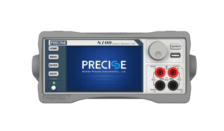
DC l-V Characteristic Test System Based on S/CS Series Source measure Meter
The whole set of test system is based on Precise S/CS series source measure meter, with probe station and special test software, it can be used for GaN HEMT, GaAs RF device DC parameter test, including threshold voltage, current, output characteristic curve, etc.
S/CS Series DC Source measure Meter
The S series source measure meter is the first localized source measure meter with high precision, large dynamic range and digital touch that PRECISE has built for many years. It integrates various functions such as input and output of voltage and current, and measurement. The maximum voltage is 300V, and the maximum current is 1A. Support four-quadrant work, support linear, logarithmic, custom and other scanning modes. It can be used for the DC l-V characteristic test of GaN and GaAs RF materials in production and R&D, as well as chips.
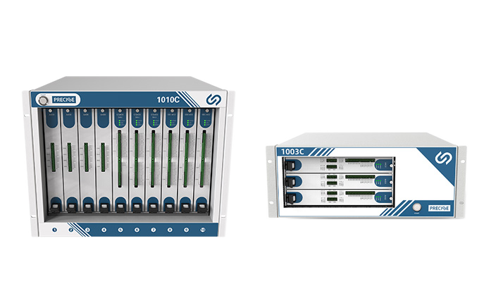
CS series plug-in source measure meter (host + sub-card) is a modular test product launched for multi-channel test scenarios. Up to 10 sub-cards can be selected for the Precise plug-in source measure device, which has multiple functions such as voltage and current input and output, and measurement. The maximum voltage is 300V, the maximum current is 1A, supports four-quadrant work, and has high channel density. , Strong synchronous triggering function, high efficiency of multi-device combination, etc.
For the DC characteristic test of RF devices, the gate voltage is generally within ±10V, and the source and drain voltages are within 60V. In addition, since the device is a three-port type, at least 2 S source measure units or 2-channel CS daughter cards are required.

Output characteristic curve test
In the case of a certain gate and source voltage VGs, the change curve between the source and drain current lbs and the voltage Vos is called the output characteristic curve. With the increase of Vos, the current los also increases to a saturated state. In addition, by testing different gate and source voltage Vcs values, a set of output characteristic curves can be obtained.
Transconductance test
Transconductance gm is a parameter that characterizes the control ability of the device gate to the channel. The larger the transconductance value, the stronger the control ability of the gate to the channel.
It is defined as gm=dlDs/dVgo. Under the condition of constant source and drain voltages, the change curve between source and drain current lDs and gate and source voltage VGs is tested, and the transconductance value can be obtained by deriving the curve. Among them, the place where the transconductance value is the largest is called gm,max.
Pulse I-V characteristic test system based on precise Р series pulse source measure meter/CP series constant voltage pulse source
The whole set of test system is based on Psys P series pulse source measure unit meter/CP constant voltage pulse source, with probe station and special test software, it can be used for GaN HEMT, GaAs RF device pulse I-V parameter test, especially the drawing of pulse I-V output characteristic curve .
P series pulse source measure meter
P series pulse source measure meter is a pulse source measure meter with high precision, strong output and wide test range launched by PRECISE, which integrates multiple functions such as input and output of voltage and current, and measurement. The product has two working modes of DC and pulse. The maximum output voltage is 300V, the maximum pulse output current is 10A, the maximum voltage is 300V, and the maximum current is 1A. It supports four-quadrant operation and supports linear, logarithmic, custom and other scanning modes. It can be used for pulsed l-V characteristic test of GaN and GaAs radio frequency materials and chips in production and research and development.
CP series pulse constant voltage source
Precise CP series pulse constant voltage source is a narrow pulse width, high precision and wide range plug-in card type pulse constant voltage source launched by Wuhan Precise Instrument. The device supports narrow pulse voltage output, and simultaneously completes output voltage and current measurement; supports multi-device triggering to realize pulse l-V scanning of devices, etc.; supports output pulse timing (such as delay.pulse width, period, etc.) adjustment, and can output complex curves. Its main features are: large pulse current, up to 10A; narrow pulse width, down to 100ns; support DC and pulse voltage output modes; support linear, logarithmic and custom multiple scanning working modes. The product can be applied to the I-V test of high-speed devices made of Nitride, Arsenide and other materials.
For the pulsed l-V characteristic test of RF devices, the gate voltage is generally within ±10V, the source and drain terminal voltages are within ±60V, the pulse width ranges from 0.5us to 500us, and the duty cycle is 10% or 20%. . In addition, since the device is a three-port type, at least two Р source measure meters or 2-channel CP daughter cards are required.

Pulse output characteristic curve test
Due to the limitations of GaN device materials and production processes, there is a current collapse effect. Therefore, there will be a power drop when the device works under pulsed conditions, and the ideal high-power working state cannot be achieved. The pulse output characteristic test method is to apply a periodic pulse voltage signal to the gate and drain of the device synchronously, and the voltage of the gate and drain will alternately change between the static operating point and the effective operating point synchronously. When Vcs and Vos are effective voltages, the current of the device is monitored. The research proves that different quiescent operating voltages and pulse widths have different effects on the current collapse.
Pulse S parameter test system based on Precise CP series constant voltage pulse source
The entire test system is based on the Pousse CP series constant voltage pulse source, with network analyzer, probe station, Bias-tee fixture, and special test software. On the basis of DC small signal S parameter test, pulse S parameter test of GaN HEMT and GaAs RF devices can be realized.
Summarize
Wuhan Precise has been focusing on the development of electrical performance test instruments and systems in the field of power devices, radio frequency devices and the third generation semiconductor. Pulse large current source, high-speed data acquisition card, pulse constant voltage source and other instrument products and a complete set of test systems. Products are widely used in the field of analysis and testing of power semiconductor materials and devices, radio frequency devices, and wide bandgap semiconductors. According to the needs of users, we can provide comprehensive solutions for electrical performance testing with high performance, high efficiency and high cost performance


 Email
Email
 Contact
 Inquiry
 Home
Home
